Today I learned how to make PCBs. I didn’t invent anything here, this is all pretty well known by the PCB-making community, but it’s not well-known to me. So I taught myself a bit!
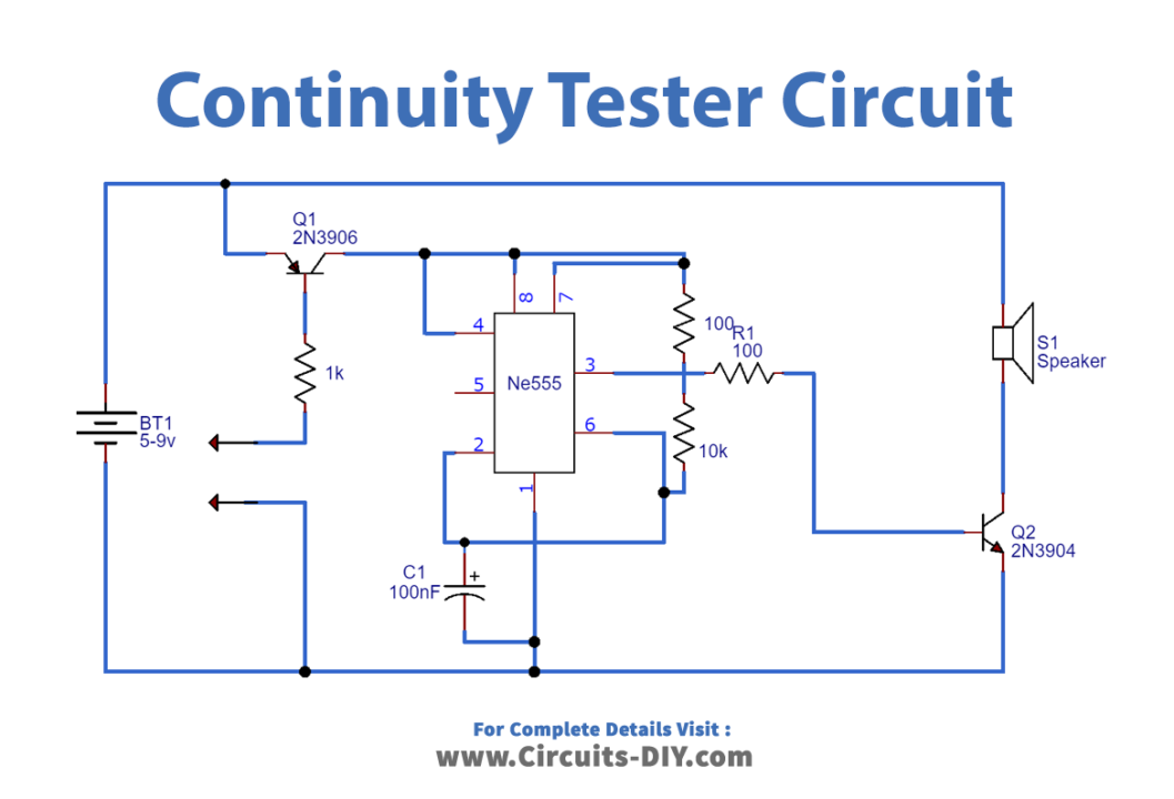
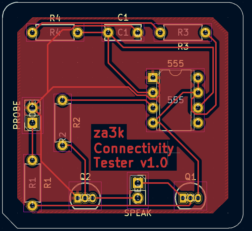
The first part was the design an electronic circuit. I decided I was short on time, so I grabbed an existing schematic.
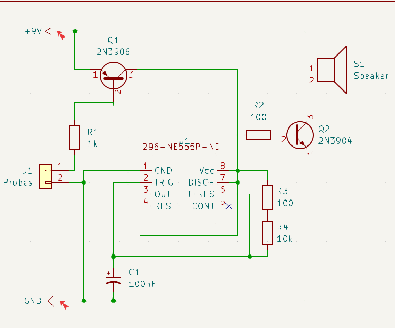
Next, I downloaded KiCAD, and recreated the circuit there. I found this video tutorial very helpful to learn kicad.
Next, I made the actual PCB layout.
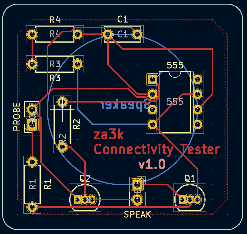
To my surprise, after a little jiggling I got it down to a one-layer design.
That means home-printing would be much easier. No having to line up the two sides carefully.
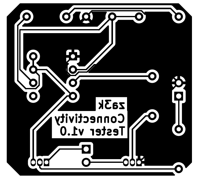
I printed out the image on paper (backwards) on my toner printer, and taped it to the copper-clad PCBs.
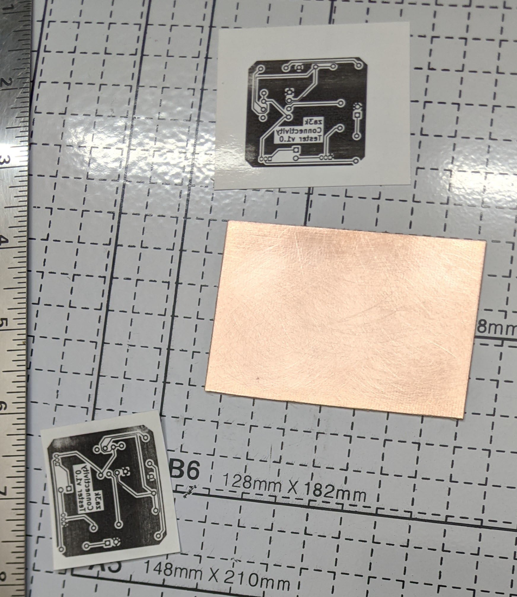
First, I tried laminating it. Almost no ink transferred, and the paper came off easily. Then I tried ironing it, but the paper stick to the iron and not to the PCB. The tape melted on the iron. For both, I dunked them in water after, which is supposed to help loosen the paper.
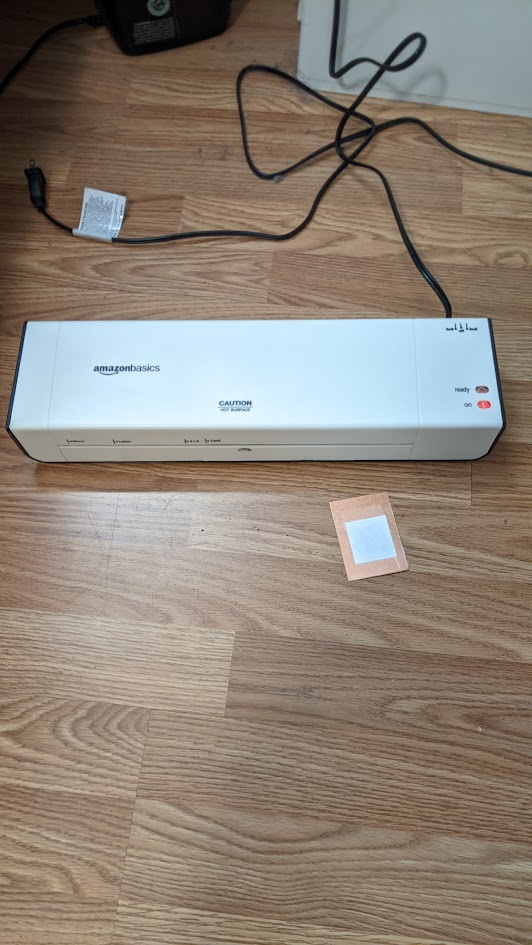
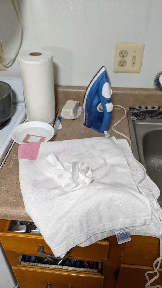
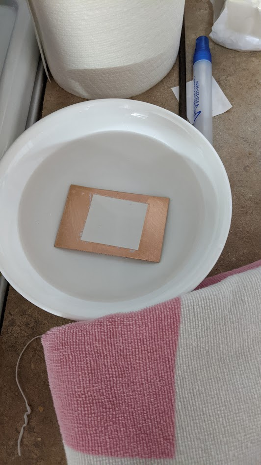
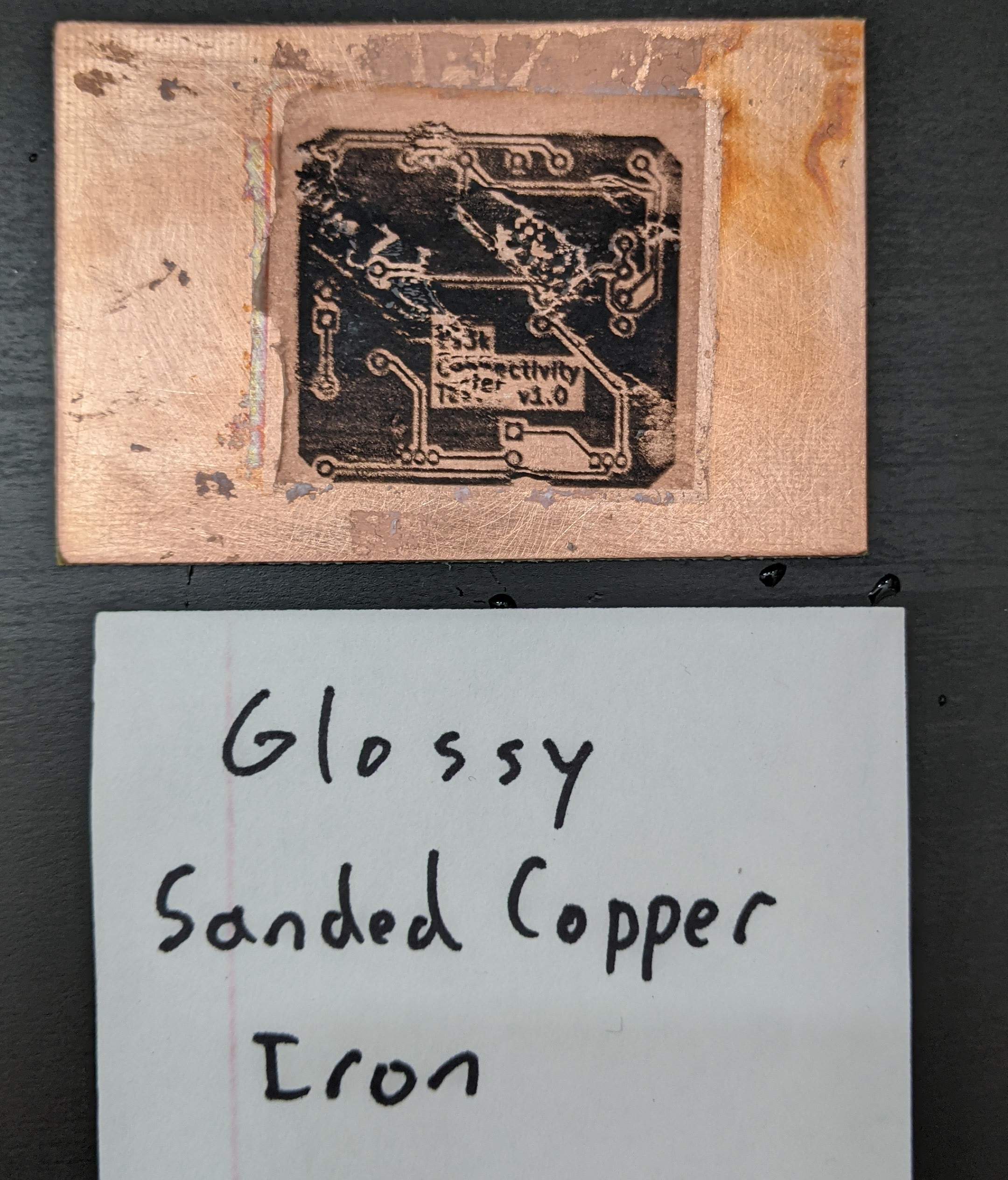
Next, I tried the standard advice–sand the PCBs (I used 320 grit) and use glossy paper. This time, both pieces of paper stuck very well. I was wary about the iron coming off again, so I just left it on place on the highest heat–this worked fine for adhesion, but I had to iron out wrinkles at the end. The laminated piece had lose edges, while the ironed piece was on there totally flat.
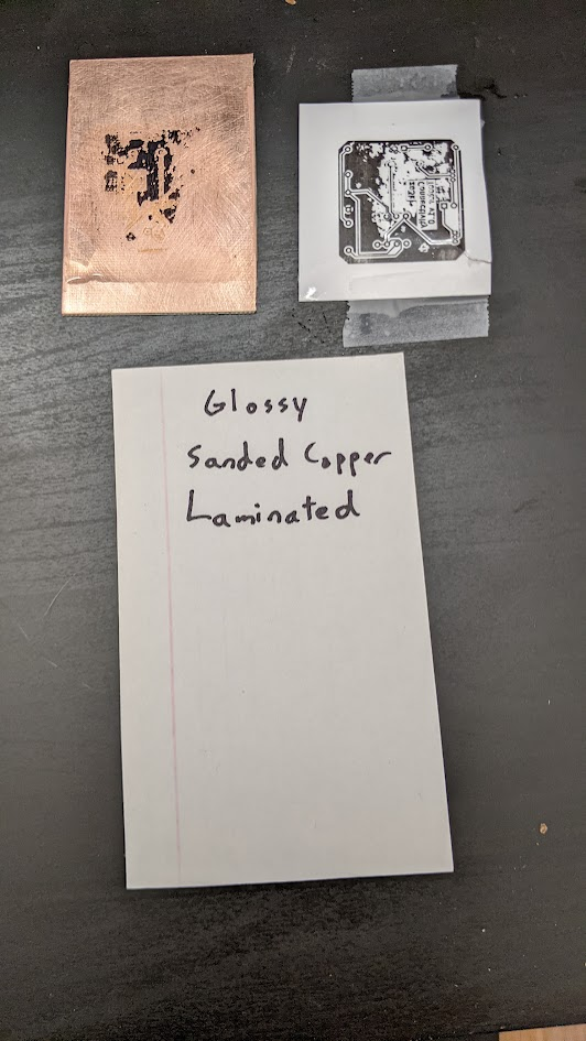
I tried peeling off the laminated paper–oops! It peeled back and most of the ink stayed on the paper. I think if I took it off more carefully, it would have worked.
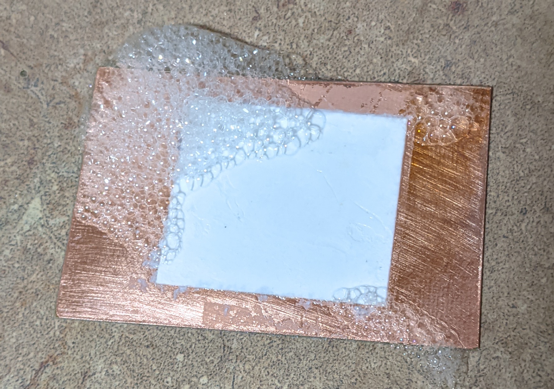
I picked at the ironed paper a bit, but it didn’t budge. I let it sit in dish soap for a while so the paper would fall apart. The first hour didn’t do anything.
Meanwhile, I made an order at PCBWay. It’s still under review.
Edit: after some advice from a friend, I peeled off this paper more aggressively, and scrubbed it off. The ink was fine. It doesn’t look great, but I think this is mostly the wrinkles during transfer. It’s a little blurry, I’ll have to do a third attempt before I try etching.